Flexible PCB
Description
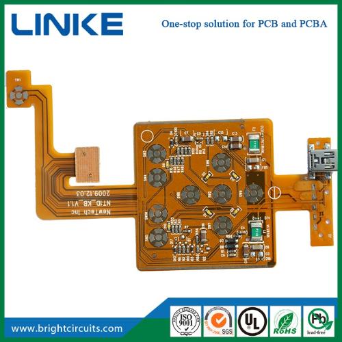
Flexible circuit boards, also known as "flexible boards", are printed circuits made of flexible insulating substrates. Flexible circuits provide excellent electrical performance, can meet the design needs of smaller and higher density installations, and also help reduce assembly processes and enhance reliability.
- Printed circuits
- Flexible circuit board
- Flexible PCB
- Flexible board
Similar products

BERATRONIC GMBH
Germany

Technical data •Max. Panel size up to 1500mm x 670mm •PCB thickness from 0.1-17.5mm •Smallest hole 0.075mm •Smallest trace/spacing 50µm •Copper layer up to 1000µm •Number of layers up to 58 •Aspect Ratio 20:1 •Rigid flex and flex •Viaplugging •Impedance control •Laser Microvias •Blind, Buried Vias Basic material •FR4, FR4 High TG, FR4 •halogen-free, CEM1/3, Rogers, •Ceramic (Al2O3), polyimide and others Surface •HAL lead-free, HAL Pb/Sn, chem. Ni/Au (ENIG), chem. Ni/Pd/Au (ENEPIG), chem. Sn, chem. Ag, OSP(Entek), galv. Ni/Au, Carbon, Ag/Pt (thick film technology) and others Solder resist and placement printing •Different paint systems (including halogen-free) and colors Standards •ISO 9001:2015 / IATF 16949 •UL listing •RoHS / REACH •Manufacturing according to IPC A600 class 2 and 3 Delivery times •Rush service from 1 AT •Series from 10 AT Data preparation •Legacy document preparation •Scan Service •Data conversion •CAM data preparation •CAD layout service

SILGA SPA
Italy
To effectively respond to the technological expectations of its customers and satisfy the different market needs, Silga is able to offer a wide and complete range of products ranging from printed circuits with standard characteristics to highly complex ones. Silga offers single-copper flexible PCBs , double-sided flexible PCBs with metalized holes (PTH), flex therm for heat dissipation, Gigaflex for the sensorized connection of the battery pack to the BMS in e-vehicles and Flexible Heaters for heating and removal of the condensation. Silga flexible PCBs find application in numerous sectors such as automotive, EMS, industrial, medical and wearable.
XIAMEN NINESUN IMP. & EXP. CO., LTD
China
Processing Technology: Electrolytic Foil Base Material: Copper Insulation Materials: Epoxy Resin Certification: UL, RoHS, ISO9001, Ts16949 Transport Package: by Vacuum Packing in Cartons Specification: UL, ROHS, SGS Origin:China HS Code: 85340090 Min. Order: 100 Pieces Port: China Production Capacity:100000 Square Meters Per Month Payment Terms: L/C, T/T, D/P Type: Rigid Circuit Board Dielectric:FR-4 Material: Fiberglass Epoxy Application: Consumer Electronics Flame Retardant Properties: V0 Mechanical Rigid: Rigid
DAMEKS
Poland
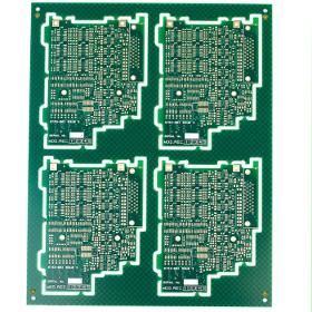
PCB depanelization is a process step in the production of large-scale assembly of electronics. To increase the throughput of printed circuit board (PCB) and surface mount (SMT) production lines, printed circuit boards are often designed to consist of many smaller individual printed circuit boards that will be used in the final product. This PCB cluster is called a panel or multi-block. The large panel is broken or "depanellated" as a process step - depending on the product, this can be right after the SMT process, after the in-circuit test (ICT), after soldering through-hole components, and even just before the final assembly of the PCBA in the enclosure.
Request for quotes
Create one request and get multiple quotes form verified suppliers.
- Only relevant suppliers
- Data privacy compliant
- 100% free