SENKENTEK PCB CO.,LTD
China
Manufacturer/ Producer
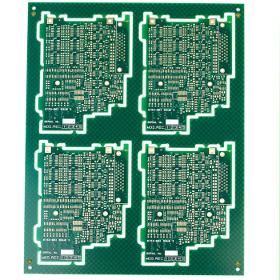
We are the PCB manufacturer with TS16949 & ISO 14001 certification and looking forward to provide the Best Solutions and Best Services & Cost-Competitive for your product. Senkentek have a strong capability and is able to provide the best quality for you. We currently serving many customers in the automotive area for many years (such as the Saint-Gobain Sekurit International, FEW GmbH, IGT). we hope to build up a long terms and fruitful co-operation with you. Senkentek is a leading worldwide provider of simple PCB to complex multi-layer printed circuit boards (PCBs). We do PCBS of Rigid PCB (4~50L), FPC (1~8L) and Rigid-flex (2~20L) . We supply our products to the various market, such as Audio, VTR, Video, digital Camera, Telecommunication, Computer, Automobile dashboards. Multi-layer Printed Circuit Board of Communications and Computer Accessories, RAM Module P.C.B., Mother Board for Computer & Industrial Computer, Interface Cards, CPU Cards, Network Cards, Modem Cards & Control Card
Website
Manufacturer/ Producer
East Industrial Zone,Nanshan District Shenzhen,Guangdong
518000 Shenzhen - China
Company info
Key figures
-
- Company headcount
- 201 – 500
-
- Sales staff
- 201 – 500
-
- % of export sales
- 100%
Organisation
-
- Year established
- 2005
-
- pages.epage-home.site-status
- Registered office – Parent company
-
- Main activity
- Manufacturer/ Producer
Business info
Trading areas
- European
- International
Payment methods
- Credit card - Cash - Cheque
- Telex transfer
- Cash on delivery
Banks
- Shenzhen Development Bank
Delivery areas
Terms of delivery (incoterms)
- Purchaser
- Shared
- Vendor
Activities of SENKENTEK PCB CO.,LTD
- Printed circuits
- PCB burn in board
- FPC manufacturer
europages also recommends
A selection of companies related to the activity:
A selection of products that might interest you
XIAMEN NINESUN IMP. & EXP. CO., LTD
China

Processing Technology: Electrolytic Foil Base Material: Copper Insulation Materials: Epoxy Resin Certification: UL, RoHS, ISO9001, Ts16949 Transport Package: by Vacuum Packing in Cartons Specification: UL, ROHS, SGS Origin:China HS Code: 85340090 Min. Order: 100 Pieces Port: China Production Capacity:100000 Square Meters Per Month Payment Terms: L/C, T/T, D/P Type: Rigid Circuit Board Dielectric:FR-4 Material: Fiberglass Epoxy Application: Consumer Electronics Flame Retardant Properties: V0 Mechanical Rigid: Rigid

BERATRONIC GMBH
Germany
Our services •Layout creation •Material procurement •SMD assembly •Manual and semi-automatic •Mounting •Reflow and wave soldering •Selective soldering •Automatic Optical Inspection (AOI) •X-ray inspection •System assemblies •In circuit tests and •Function test •Revision and repair •Rework Station •Short delivery times
BERATRONIC GMBH
Germany
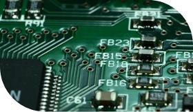
Technical data •Max. Panel size up to 1500mm x 670mm •PCB thickness from 0.1-17.5mm •Smallest hole 0.075mm •Smallest trace/spacing 50µm •Copper layer up to 1000µm •Number of layers up to 58 •Aspect Ratio 20:1 •Rigid flex and flex •Viaplugging •Impedance control •Laser Microvias •Blind, Buried Vias Basic material •FR4, FR4 High TG, FR4 •halogen-free, CEM1/3, Rogers, •Ceramic (Al2O3), polyimide and others Surface •HAL lead-free, HAL Pb/Sn, chem. Ni/Au (ENIG), chem. Ni/Pd/Au (ENEPIG), chem. Sn, chem. Ag, OSP(Entek), galv. Ni/Au, Carbon, Ag/Pt (thick film technology) and others Solder resist and placement printing •Different paint systems (including halogen-free) and colors Standards •ISO 9001:2015 / IATF 16949 •UL listing •RoHS / REACH •Manufacturing according to IPC A600 class 2 and 3 Delivery times •Rush service from 1 AT •Series from 10 AT Data preparation •Legacy document preparation •Scan Service •Data conversion •CAM data preparation •CAD layout service
DAMEKS
Poland
PCB depanelization is a process step in the production of large-scale assembly of electronics. To increase the throughput of printed circuit board (PCB) and surface mount (SMT) production lines, printed circuit boards are often designed to consist of many smaller individual printed circuit boards that will be used in the final product. This PCB cluster is called a panel or multi-block. The large panel is broken or "depanellated" as a process step - depending on the product, this can be right after the SMT process, after the in-circuit test (ICT), after soldering through-hole components, and even just before the final assembly of the PCBA in the enclosure.
Request for quotes
Create one request and get multiple quotes form verified suppliers.
- Only relevant suppliers
- Data privacy compliant
- 100% free